arrow-left-2arrow-left-3arrow-left-4arrow-leftchronodiggdown-arrow--lineardown-arrowearthenvelopefacebookfacebook_ (2)facebook_forward-arrowforwardgooglehomeico-downloadico-linkindustries--1industries--10industries--10_oldindustries--2industries--3industries--4industries--5industries--6industries--6_oldindustries--7industries--8industries--9linkedinmailmarkernewspaperpadlockpage-arrow-leftpage-arrow-rightpage-listpencilpinterestplay-buttonprintersearchsocial-diggsocial-facebooksocial-googlesocial-instagramsocial-linkedinsocial-pinterestsocial-twittersocial-youtubestartelephonetwittertwitter_user

Semiconductor and sapphire wafers's lapping, polishing and CMP processes

This process is particularly critical since strict control of wafer total thickness variation and surface finishing is required. 

Semiconductor and sapphire wafers's lapping, polishing and CMP precesses
DESCRIPTION

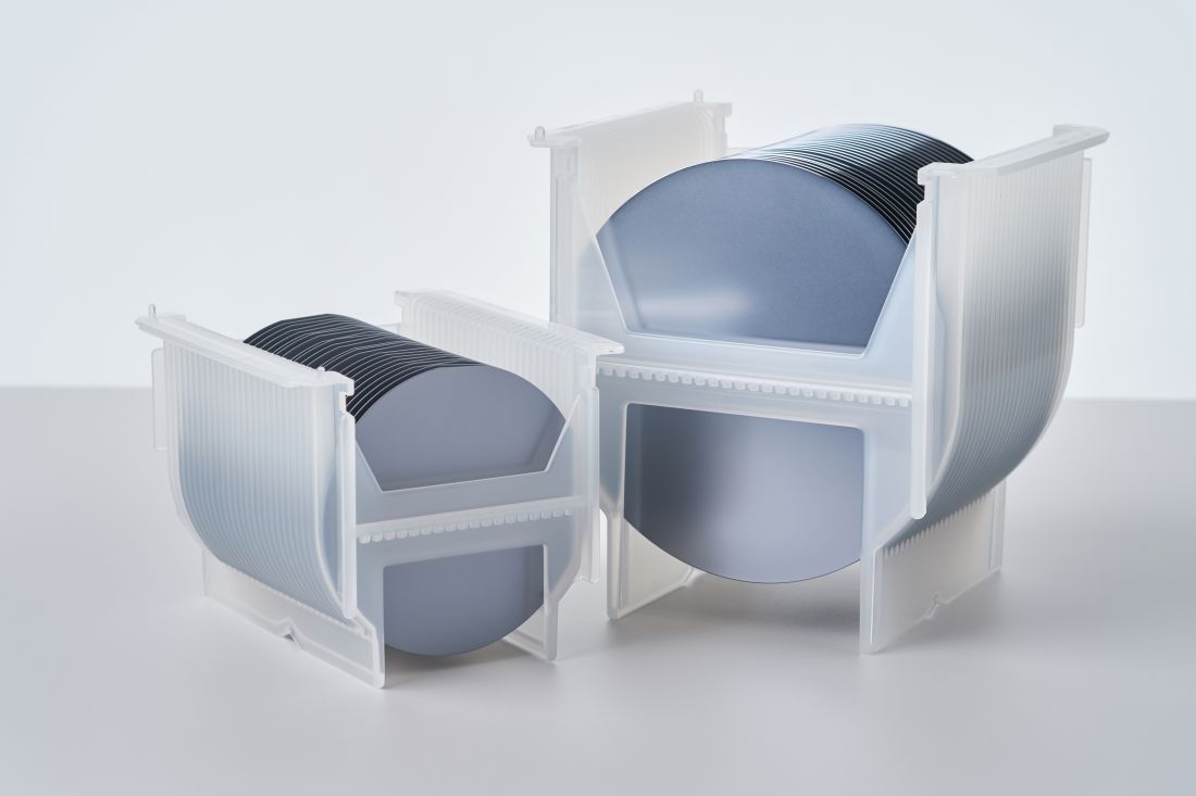
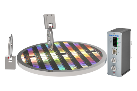
Wafers made of silicon, sapphire, gallium arsenide, silicon carbide and other materials, require high-precision surface processing technology. Grinding, lapping, mechanical and chemical polishing machines for substrates of all diameters have to provide high process results that define the leading edge regarding local and global geometries.

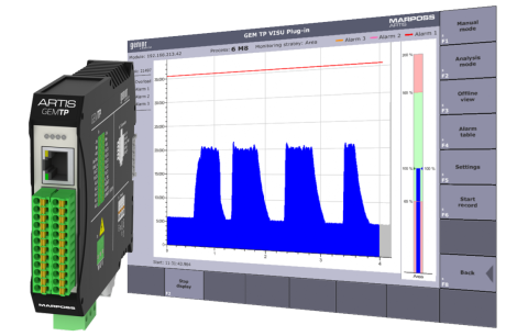
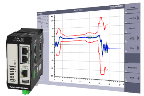
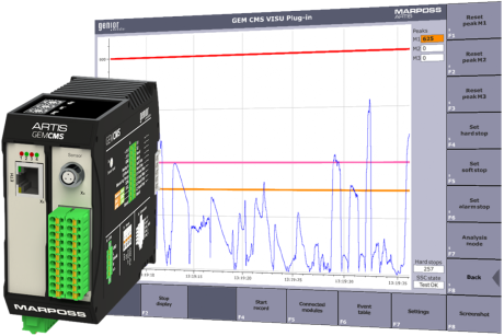
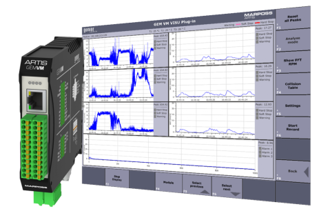
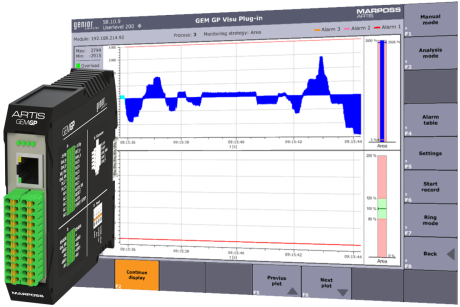
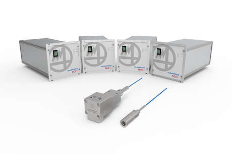
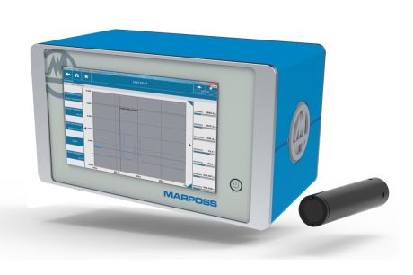
Lapping and polishing are critical: they require time-consuming steps and strict control of wafer total thickness variation. Thanks to the Marposs infrared sensor, it is possible to control the thickness during and immediately after this crucial operation. That helps keep the process under control regardless of wear  on consumable parts.  The Marposs monitoring sensor, instead, can keep unwanted vibrations under control. 

BENEFITS
  • Absolute thickness measure of Si-Sapphire-SiC-GaN wafers during lapping with nanometric resolution
  • Thickness control during the entire machining cycle, allowing to stop machining at the right  time
  • Measure independent of pad wearing  over time
  • Vibration monitoring for a perfect surface finishing
Download

BROCHURES AND MANUALS

Brochure
English SEMICONDUCTORS: (2.27MB)
Italian SEMICONDUCTORS: (2.63MB)
German SEMICONDUCTORS: (2.28MB)
Russian SEMICONDUCTORS: (2.23MB)
Japanese SEMICONDUCTORS: (2.38MB)
Korean SEMICONDUCTORS: (7.41MB)
Simplified Chinese SEMICONDUCTORS: (5.06MB)
Close
Close

Request information

Insert your first name
Insert your last name
Insert the company name
Insert your email

To help the message delivery directly to the division in charge, please select the application field in the list below:

Insert your message

Before sending the form please read carefully the INFORMATION NOTICE on personal data processing provided in accordance with the Regulation EU 2016/679.

Please accept the privacy policy
Top Contact us