arrow-left-2arrow-left-3arrow-left-4arrow-leftchronodiggdown-arrow--lineardown-arrowearthenvelopefacebookfacebook_ (2)facebook_forward-arrowforwardgooglehomeico-downloadico-linkindustries--1industries--10industries--10_oldindustries--2industries--3industries--4industries--5industries--6industries--6_oldindustries--7industries--8industries--9linkedinmailmarkernewspaperpadlockpage-arrow-leftpage-arrow-rightpage-listpencilpinterestplay-buttonprintersearchsocial-diggsocial-facebooksocial-googlesocial-instagramsocial-linkedinsocial-pinterestsocial-twittersocial-youtubestartelephonetwittertwitter_user

Wafers Metrology Machines

Metrology and wafer defects detection is vital in semiconductor manufacturing, providing the means to monitor and control the quality of each step in the manufacturing sequence.

Wafers metrology machines
DESCRIPTION

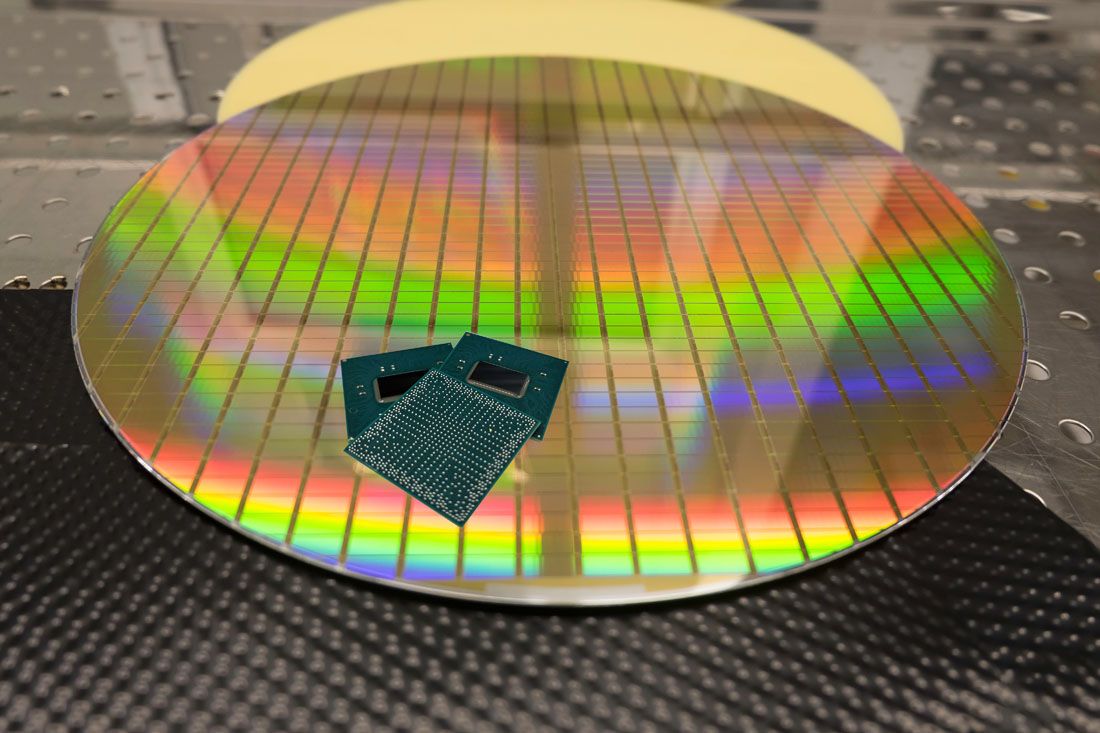
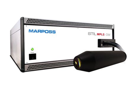
Marposs and STIL sensors cover many applications, starting from thickness, TTV, bow, and warp measures until a complete 2D image and 3D topography.

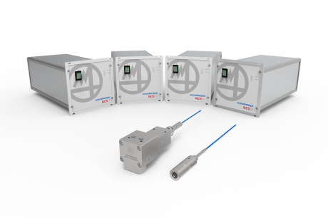
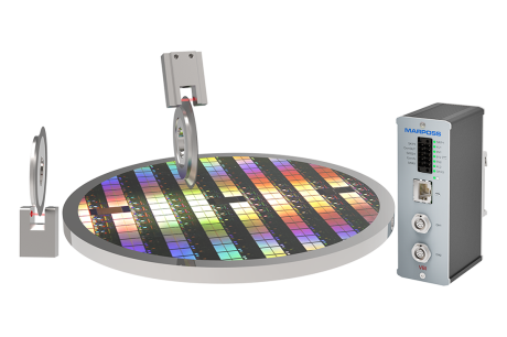
Chromatic Confocal technology is the optimized solution to produce high-accuracy bump measurements. Optical pens offer different working distance, measurement range, spot sizes  and numerical apertures to better suit the application requirements. Interferometric products (IR and white light) are also available to detect the thickness of transparent and non-transparent materials performing very accurate measures.

Line sensors also allow 3D imaging: coaxial acquisition over a defined line length is performed at a high-frequency while maintaining the advantage of a large depth of focus and high numerical aperture.

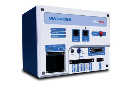
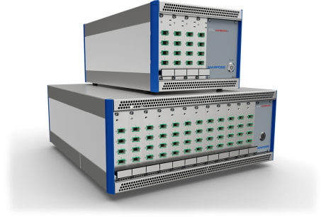
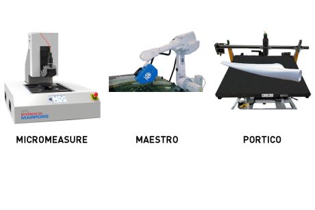
All these types of sensors can be integrated inside metrology and inspection machines. The decades of experience of Marposs and STIL’s are available for a customized solution and dedicated optical design.

BENEFITS
  • Lateral Resolution < 1μm
  • High Slope Angle: +/-45° with NA of 0.75
  • Up to 360.000 Measured points/second in sub-micrometric accuracy and nanometric resolution in Z-axis
  • Bumps measurement using CLMG / EVEREST sensors
  • The position of measuring points can be on a line or defined by the customer
  • Extended depth of field (of perfect focus)
Download

BROCHURES AND MANUALS

Brochure Data Sheet
English SEMICONDUCTORS: (2.27MB)
STIL - General Catalogue: (13.23MB)
-
Italian SEMICONDUCTORS: (2.63MB)
-
German SEMICONDUCTORS: (2.28MB)
-
Russian SEMICONDUCTORS: (2.23MB)
-
Japanese SEMICONDUCTORS: (2.38MB)
STIL - General Catalogue: (21.22MB)
-
Korean SEMICONDUCTORS: (7.41MB)
-
Simplified Chinese SEMICONDUCTORS: (5.06MB)
STIL - General Catalogue: (18.78MB)
Close
Close

Request information

Insert your first name
Insert your last name
Insert the company name
Insert your email

To help the message delivery directly to the division in charge, please select the application field in the list below:

Insert your message

Before sending the form please read carefully the INFORMATION NOTICE on personal data processing provided in accordance with the Regulation EU 2016/679.

Please accept the privacy policy
Top Contact us