Higher yield for a highly complex production process
Placing and maintaining a process under control is the key factor for any production. This is even more true for the very demanding semiconductor and semiconductor like manufacturing processes, which can be considered some of the most complex ones, that requires the control of an increasing number of parameters. Not to forget that semiconductor is a brittle and hard material that requires dedicated machine tools to slice, lap, thin, get intelligent and finally cut the die.
In order to improve and maintain high yield, inspection and metrology are key factors. They are also crucial for the management of the semiconductor manufacturing process to find defects on both patterned and unpatterned wafers.
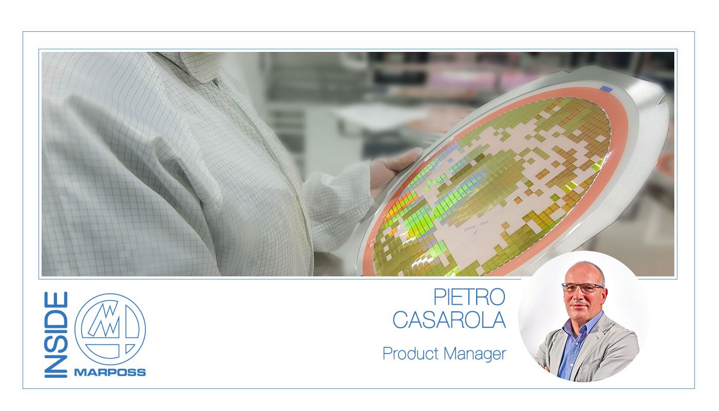
Marposs: your partner for metrology and inspection
Marposs engineers are ready to support you in defining how to improve the performances of automatic machines used during wafer processing, the front-end and back-end fabrication steps. Indeed we offer sensors and gauges for slicing and lapping machines, back grinders and dicing saws, wafer shape (bow/warp) measurements, layer & pattern measurements, bump & groove measurements.
The semiconductor and semiconductor like industries continue to produce ever smaller devices that are more complex in both shape and materials. For these purposes, Marposs has a complete range of non-contact sensors used for thin-film metrology, wafer dimensional characterization, wafer inspection and packaging inspection. Our sensors can work inside automatic inspection machines to find defects and dimensional variation.
Here some examples of how our products that can be of profitable used.
Our diamond tip for the control of the ingot slicing machine
During the sawing process, the ingots are slowly lowered and cut into wafers for several hours. The trend is to use thinner diamond wires to minimize the cutting width and then get more wafers from a single ingot with significantly faster production speed.
In case the diamond wire breaks during the ingot slicing process, it is important to stop the machine immediately. Marposs acoustic sensor can be integrated inside the ingot-slicing machine to detect the wire breakage, immediately stop the machine, and then ease the next operation of wire replacement.
Create the flawless shapes: wafer lapping machine
For wafers made of silicon, sapphire, gallium arsenide, silicon carbide and other materials, the high-precision surface processing technology is required. Grinding, lapping, mechanical and chemical polishing machines for substrates of all diameters have to provide high process results defining the leading edge in terms of local and global geometries.
This process is a particularly critical one, which requires time spending steps and strict control of wafer total thickness variation. Thanks to Marposs infrared sensor, it is possible to control the thickness during and soon after this important operation. This helps to maintain the process under control independently from the wear of the consumable parts.
Wafer back grinding machine: a matter of thickness
Achieving the correct wafer thickness before assembly is critical in semiconductor manufacturing. Wafer back grinding (or wafer thinning) is a semiconductor manufacturing process designed to control the wafer thickness, which is essential to produce ultra-thin wafers used to create stacked and high-density packaging in compact electronic devices.
Wafer thinning is always a critical process. Chips are already present on the wafer and any fail in the process affects the production yield and costs. Tight control on the thinning in-process operation is possible using contact gauges or no-contact sensors, even in presence of DI water.
Optical design for the inspection in semiconductor fabrication
Metrology and wafer defects detection are vital in semiconductor fabrication since they provide the means to monitor and control the quality of each step in the manufacturing sequence.
STIL is a brand of Marposs Group, and is world leader company in R&D, production and sales of optical measurement instruments based on chromatic confocal technology.
Marposs and STIL sensors cover a wide range of applications starting from thickness, TTV, bow, and warp measures until a complete 2D image and 3D topography.
Chromatic Confocal technology is the optimized solution to produce high-accuracy bump measurements. The optical pens offer different working distance, measurement range, spot size & numerical aperture to better suit the application requirements. Interferometric (IR and white light) products are also available to detect thickness of transparent and non-transparent materials performing very accurate measures.
Line sensors then permit to obtain 3D images: coaxial acquisition on a defined line length is performed at high-frequency rate keeping the advantage of a large depth of focus and a high numerical aperture.
For microscopy purposes, 2D chromatic confocal line cameras are also available. For applications where the very high-resolution and extended depth of focus are required, these allow to obtain a perfect focus on the Z-axis.
That's what makes them the right solution to inspect possible defects for instance on the wafer edge and during the packaging process.
All these types of sensors can be integrated inside metrology and inspection machines. Marposs and STIL decades of experience are available for a customized solution and dedicated optical design.
Discover more about Marposs solutions for the semiconductor industry.