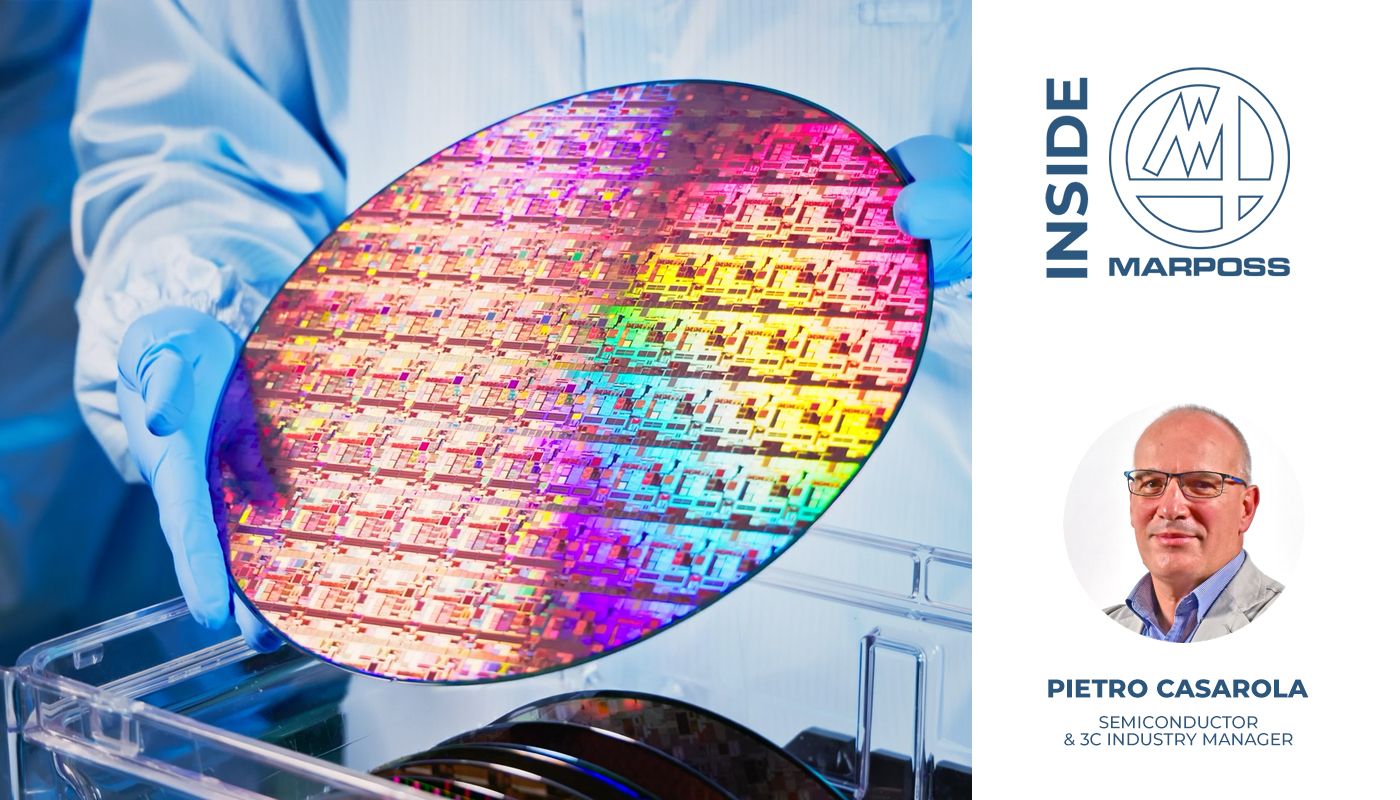
From wafer to perfection: how Marposs sensors support semiconductor quality
For more than twenty years, Marposs has been a trusted partner in delivering advanced measurement solutions for the semiconductor industry. Thanks to deep expertise in metrology and wafer inspection, we support customers in identifying the most suitable solutions for monitoring material thickness and the so-called critical dimensions throughout the chip manufacturing process.
When dealing with coatings or layers, thickness is only part of the equation. Other factors must also be considered, including the presence of additional coatings, the homogeneity of the material, and surface roughness. To address these challenges, Marposs offers thickness measurement sensors capable of covering extremely wide ranges, from just a few tens of nanometers up to one millimeter.
Our interferometric products stand out for their high signal processing speed, micrometer-sized measurement spots, high-precision optical design, and intelligent signal processing. In parallel, the confocal chromatic product line enables accurate 3D measurements of critical features such as steps, bumps, and pillars, supporting precise dimensional control across multiple applications.
Integration into production environments is equally important. Marposs controllers are equipped with advanced machine interfaces, including Fieldbus and Ethernet ports, making integration into existing systems straightforward and efficient. The interferometric sensor line can measure the thickness of substrates such as silicon, SiC, GaN, glass, and sapphire, as well as ultra-thin coatings such as silicon oxide and dielectric materials, including interlayer dielectrics.
Marposs is also a leading supplier of sensors designed for direct installation in wafer processing machines. A notable example is the back-grinding machine, widely used to thin silicon substrates during the back-end process and increasingly adopted in front-end processes after the deposition of EMC protective layers.
The built-in processing intelligence of our sensors allows thinning machines to receive stable and accurate signals from the substrate under processing, regardless of the type of chip present on the front side. Whether working with 3D or 2D chips, or DBG wafers, substrates can be accurately measured during back grinding, down to thicknesses of just a few microns.
As semiconductor technology evolves, thinner substrates are becoming essential for enabling faster and more compact chips. They also play a key role in supporting emerging design technologies such as Backside Power Delivery Networks (BSPDN) and Wafer Level Packaging (WLP).
In addition to back grinding applications, Marposs smart sensors can also be integrated into CMP machines. In this context, it is essential to monitor micrometer-scale material removal with nanometer-level accuracy. These systems are designed to maintain performance even when working with thick silicon substrates that require extremely high geometric quality and defect-free surfaces.
Thanks to their high processing speed, Marposs systems can monitor wafer processing directly inside CMP machines, even in challenging environments where slurry is present and the table is in continuous motion.
Marposs infrared and white-light interferometers can also be used in front-end processes to monitor ultra-thin coatings immediately after deposition. These include photoresists, trench depths, or TSVs with high aspect ratios, all measured with high accuracy.
To support customers at every stage, Marposs technicians are available to help identify the most suitable solution for each specific application. Support can be provided directly on-site or through dedicated testing in our laboratories. In addition, we offer custom-made products, combining mechanical, electronic, and optical design expertise to adapt our technology to individual production requirements.
DISCOVER MORE