arrow-left-2arrow-left-3arrow-left-4arrow-leftchronodiggdown-arrow--lineardown-arrowearthenvelopefacebookfacebook_ (2)facebook_forward-arrowforwardgooglehomeico-downloadico-linkindustries--1industries--10industries--10_oldindustries--2industries--3industries--4industries--5industries--6industries--6_oldindustries--7industries--8industries--9linkedinmailmarkernewspaperpadlockpage-arrow-leftpage-arrow-rightpage-listpencilpinterestplay-buttonprintersearchsocial-diggsocial-facebooksocial-googlesocial-instagramsocial-linkedinsocial-pinterestsocial-twittersocial-youtubestartelephonetwittertwitter_user

Back Grinding: Wafer Thinning

Wafer thinning is always a delicate process. Tight control on the in-process thinning operation is possible using contact gauges or non-contact sensors.

Back end: wafer thinning
DESCRIPTION

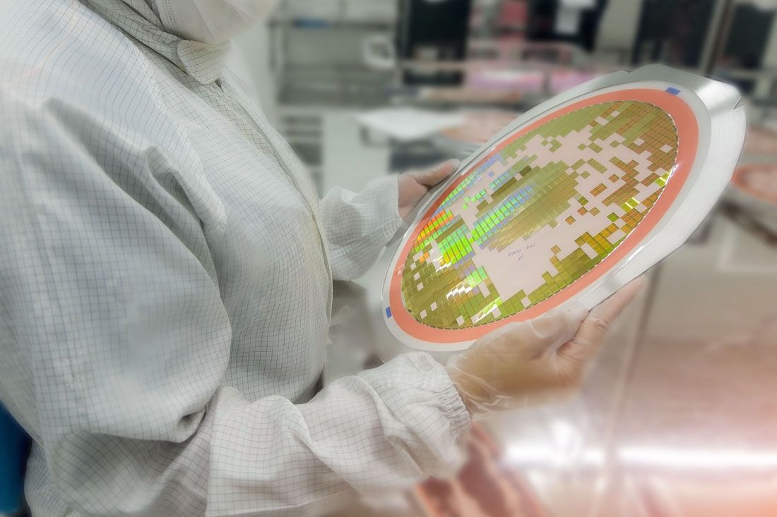
Achieving the correct wafer thickness before assembly is a key factor in semiconductor manufacturing. Wafer back grinding (or wafer thinning) is a semiconductor manufacturing process designed to control the wafer thickness, essential to produce ultra-thin wafers used to create stacked and high-density packaging in compact electronic devices.

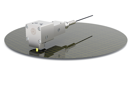
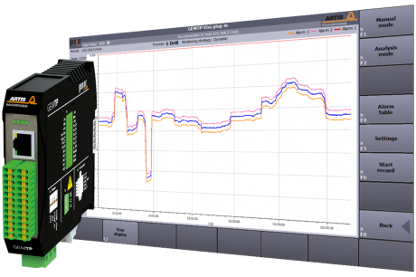
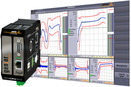
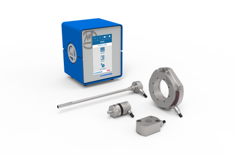
Wafer thinning is always a critical process. The chips are already on the wafer and any failure in the process affects production yield and costs. Tight in-line control on the thinning in-process operation is possible using contact gauges or non-contact sensors, even in the presence of DI water. 

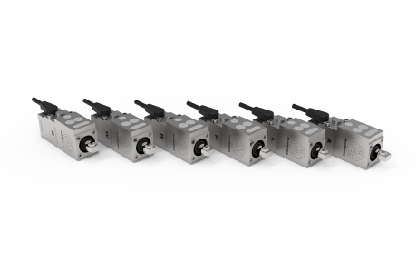
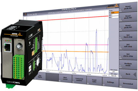
Using Marposs sensors is even possible to detect the very moment the grinding wheel touch the wafer  or check any power overload.
BENEFITS
  • In-process reliable thickness measure in a dry and wet environment
  • Measure not influenced by tape support or glue presence
  • From 4 to 900µm absolute thickness control (one side measure)
  • Smart thickness elaboration for a smooth control till very thin thickness and data-log (black box function)
     
Download

BROCHURES AND MANUALS

Brochure
English SEMICONDUCTORS: (2.27MB)
Italian SEMICONDUCTORS: (2.63MB)
German SEMICONDUCTORS: (2.28MB)
Russian SEMICONDUCTORS: (2.23MB)
Japanese SEMICONDUCTORS: (2.38MB)
Korean SEMICONDUCTORS: (7.41MB)
Simplified Chinese SEMICONDUCTORS: (5.06MB)
Close
Close

Request information

Insert your first name
Insert your last name
Insert the company name
Insert your email

To help the message delivery directly to the division in charge, please select the application field in the list below:

Insert your message

Before sending the form please read carefully the INFORMATION NOTICE on personal data processing provided in accordance with the Regulation EU 2016/679.

Please accept the privacy policy
Top Contact us